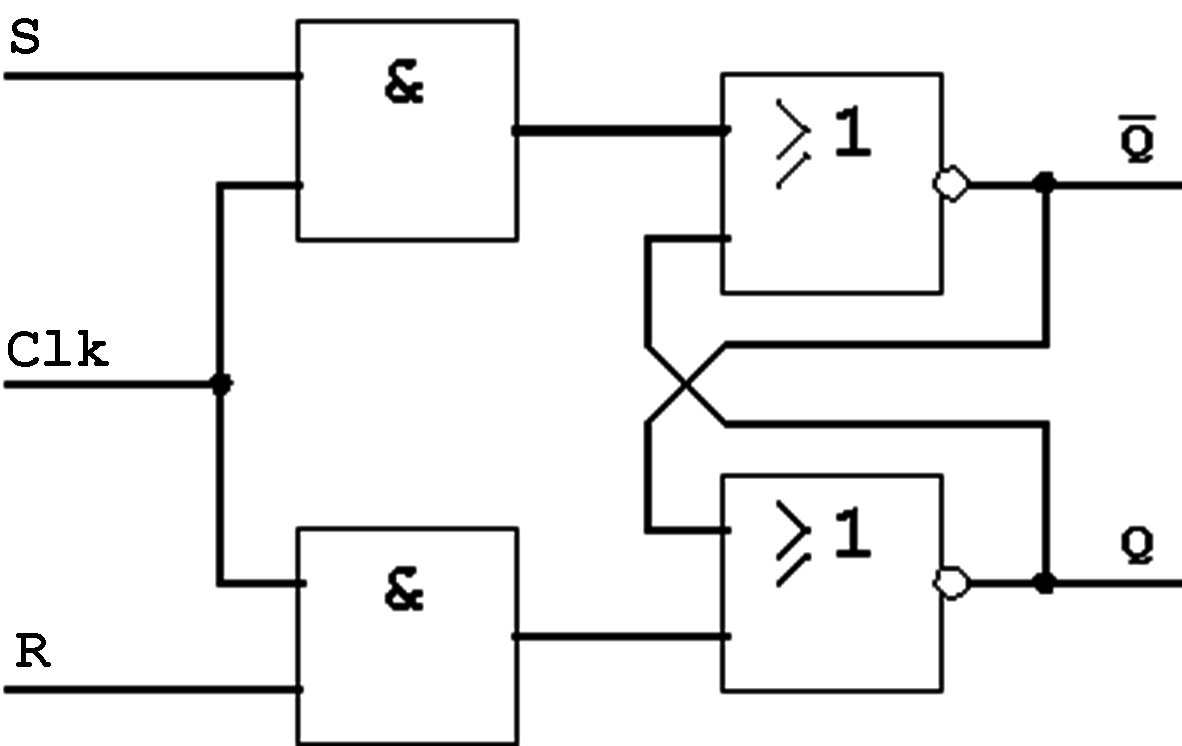
Figure 4.18: Clocked RS Flip-Flop (gated Latch).
| Contents | Previous Chapter | Next Chapter |
Characteristic for the simple RS Flip-Flop is that a change in the input parameters R and S gets evaluated immediately, which means that the Flip-Flop can accept new data at the logical inputs R and S at every time.
But in many applications it would be an advantage when the data transfer can be restricted to well defined and precisely controllable moments. Consequently the flip-flop should evaluate the logical input signals only at externally defined timing intervals.
This additional timing control is called "clock" (Clk, clock), the corresponding signal "clock signal". In its functionality this Clk input corresponds to the latch function of the elementary latch flip-flop introduced before. The flip-flop that is controlled in this way is called a "gated latch".
To transform the basic RS Flip-Flop into a gated flip-flop it is necessary to implement a clock input which can for instance fulfil the following condition:
Figure 4.18: Clocked RS Flip-Flop (gated Latch).
Now the circuit obeys the following timing signal:
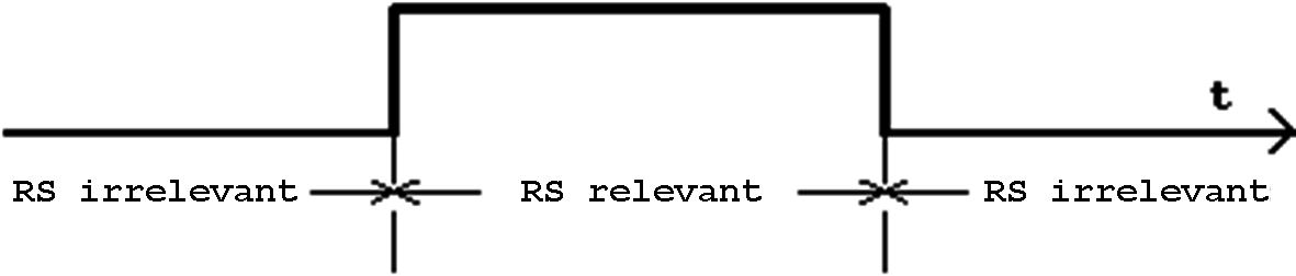
Figure 4.19: Clock signal of the gated latch.
Only during the relevant level "1" signal will be passed to the flip-flop ("1" has been chosen arbitrarily as the active level).
Such a system is called "level-sensitive" (sometimes also "level-controlled", "level-triggered"), the function level control.
Introducing the level control for the RS Flip-Flop does not remove the forbidden state (R=S="1"), but a small modification of the clocked RS Flip-Flop can solve this problem and avoid this state.
In this modified version of the RS FF the R input will be defined as the inverted form of the S input. In other words, there will be only one input signal which in this case will be named "D" (from data or delay):.
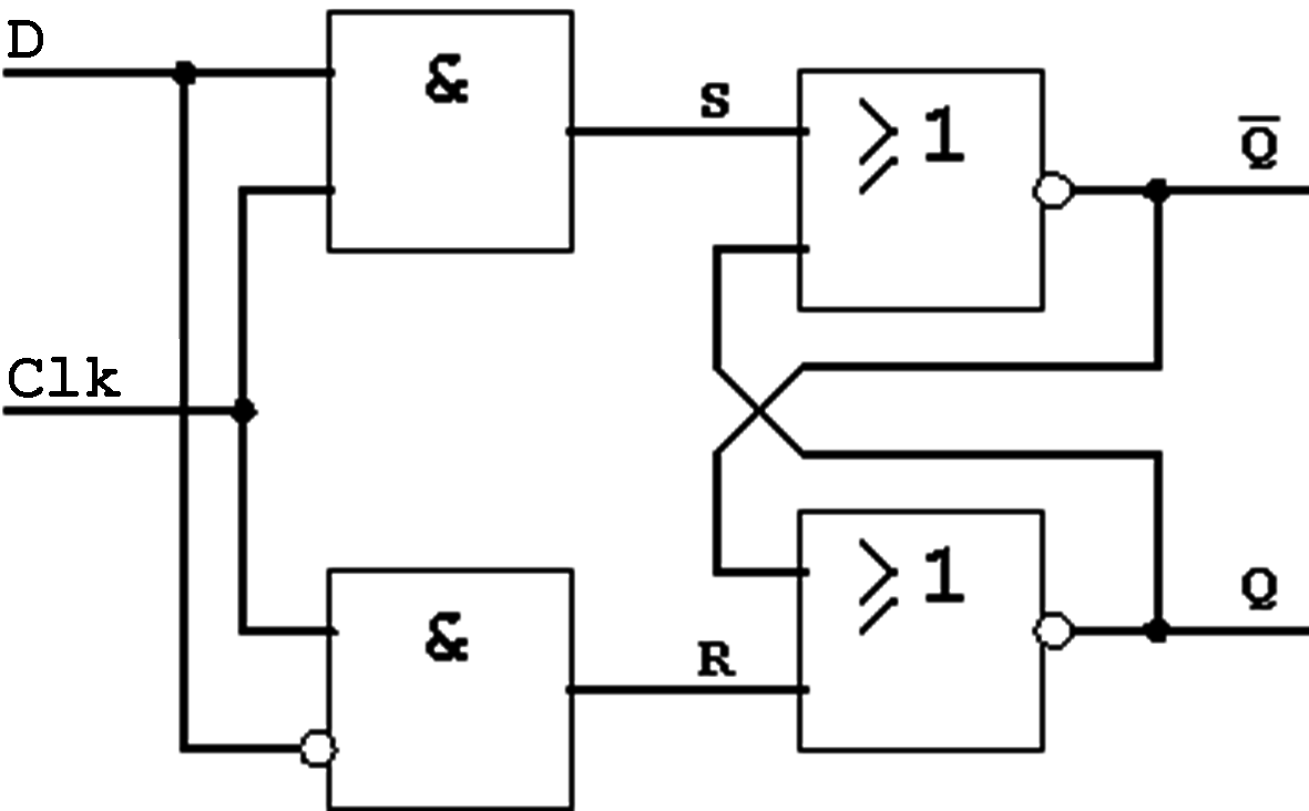
Figure 4.20: D Flip-Flop
This flip-flop formed in this way is called "D Flip-Flop".
The K-Map of the D Flip-Flop can be designed as a simplified K-Map of the RS Flip-Flop, eliminating at the same time the forbidden state:
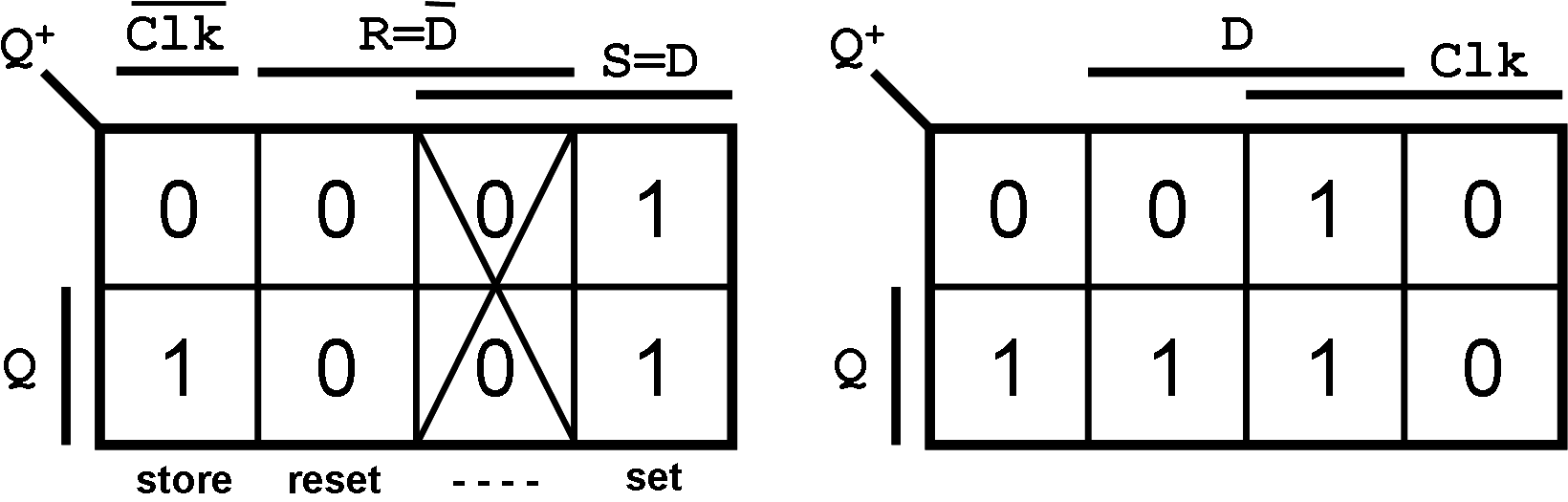
Figure 4.21: K-Map of the des D Flip-Flop.
In the circuit symbol the level triggering (control using clock level) is indicated using a rectangle:
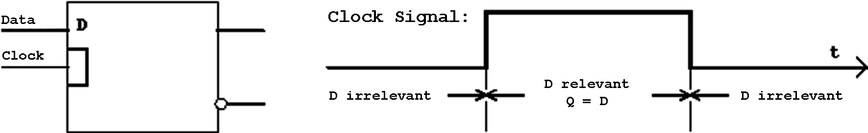
Figure 4.22: Circuit Symbol (left) and clock signal according to the K-Map.
Another solution to avoid the state which is forbidden in the RS Flip-Flop can be found by defining a new (fourth) function. This extended FF behaviour is possible by introducing an additional feedback of the flip-flop outputs. With this modification the so-called "Toggle" function is created ("change" function).
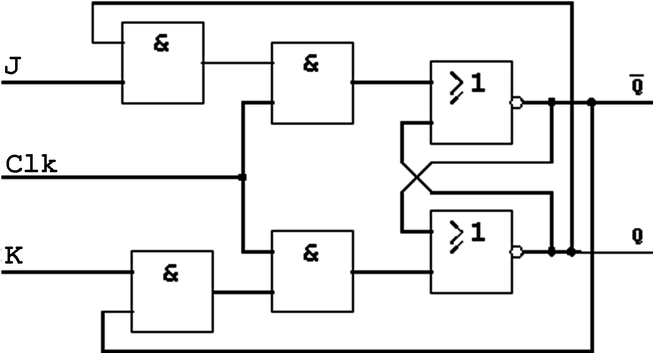
Figure 4.23: JK Flip-Flop in mixed representation (AND/NOR).
The logic inputs of this new type of flip-flop, that replace the inputs R and S, are now named J and K
(from engl. J = jump,
K = kill); this flip-flop is therefore called the JK Flip-Flop.
In the K-Map four different independent function can now be distinguished:
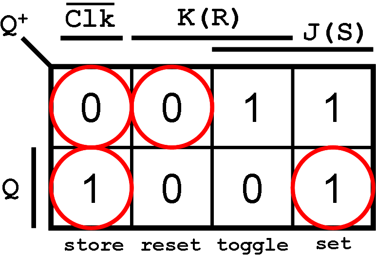
Figure 4.24: K-Map of the JK Flip-Flop with the new state "Toggle" (change).
For the functional equation of the JK Flip-Flop this results in:
| (4.4) |
 |
Table 4.5: Function Table of the JK Flip-Flop.
For practical applications the toggle mode of the output value is of special importance. Besides the function table the so-called transition table of the JK Flip-Flop is very useful in connection with this mode of operation.
| not jump |  |
|||
| jump |  |
|||
| kill |  |
|||
| not kill |  |
Table 4.6: Transition Table of the JK Flip-Flop.
(*) indicates the term of the function equation that is responsible for the transition.
The new function "toggle" results in a one-time change of the FF output values. This creates problems when clock level control is used. The truth table 4.5 assumes a combinational circuit in which the signal inputs remain stable during one timing period. But in the indicated circuit the input signal will change whenever the output signals change.
Example:
The initial situation shall be described by:
| J = K = "1" and Q = "0" | . | (4.5) |
Activating the clock pulse leads to Q = "1" (see Table 4.5). This signal change occurs after the circuit-dependent propagation delay time tp. Then the new situation will be
| J = K = "1" and Q = "1" | . | (4.6) |
When the clock input remains open the process is repeated. A continuing change between Eq. 4.5 and Eq. 4.6 will occur. Consequently the output signal Q will oscillate between "0" and "1".
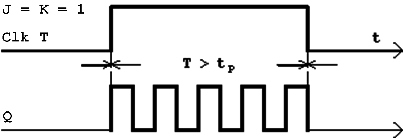
Figure 4.25: JK Flip-Flop with "race-around" Oscillations.
This behaviour called "race-around" can only be avoided when the control is done with clock pulses that are short in comparison to the FF propagation delay time tp.
In order to be able to use clock pulses of finite length and at the same time meet the demand for a single change, the so-called clock edge triggering is introduced. This type of control defines an active edge, that defines the exact moment when the logical input signals are evaluated.
Edge control (triggering) can be implemented in a very simple way, connecting two level triggered JK or RS flip-flops in series.
Master 4.26: Master-Slave Configuration of two Flip-Flops (JK/RS).
Arrangements of this type are called "Master-Slave" circuits, because the first FF is completely controlling (master function) the second one.
The functionality of this flip-flop can be divided into four phases:
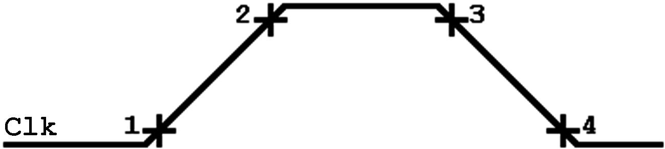
Figure 4.27: Clock Pulse.
|
In the arrangement shown here the effective signal change occurs at the Q outputs with the trailing clock edge (1 --> 0).
Flip-Flops that are controlled by one edge of the clock signal are called "single-edge triggered" (single-edge sensitive) flip-flops.
Definition:
4.4.4.1 Construction of Master-Slave Flip-Flops
Edge-triggered Master-Slave Flip-Flops can be implemented according to Fig. 4.26 using two JK Flip-Flops. But they can also be constructed in the corresponding way connecting two RS Flip-Flops.
Fig. 4.28 shows an MS Flip-Flop realization (RS MS-FF, master-slave) using RS Flip-Flops. For this flip-flop, too, the additional condition to avoid the forbidden state has to be observed.
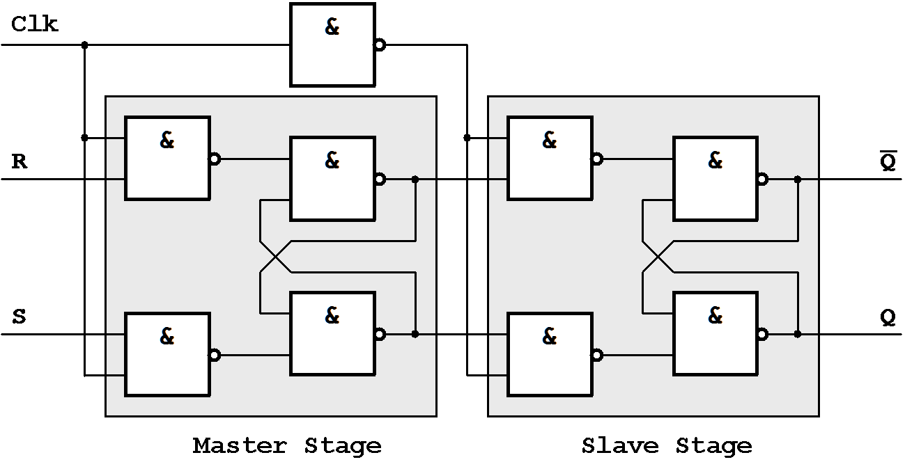
Figure 4.28: Complete RS Master-Slave Flip-Flop (in NAND realization).
An equivalent JK Flip-Flop realization is shown in Fig. 4.29:
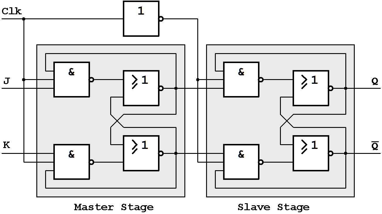
Figure 4.29: Complete JK Master-Slave Flip-Flop (in mixed realization).
This configuration is also following the block diagram of Fig. 4.26.
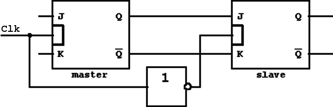
More common is the following MS construction, in which the required feedbacks are leading from the Slave outputs to the Master inputs:
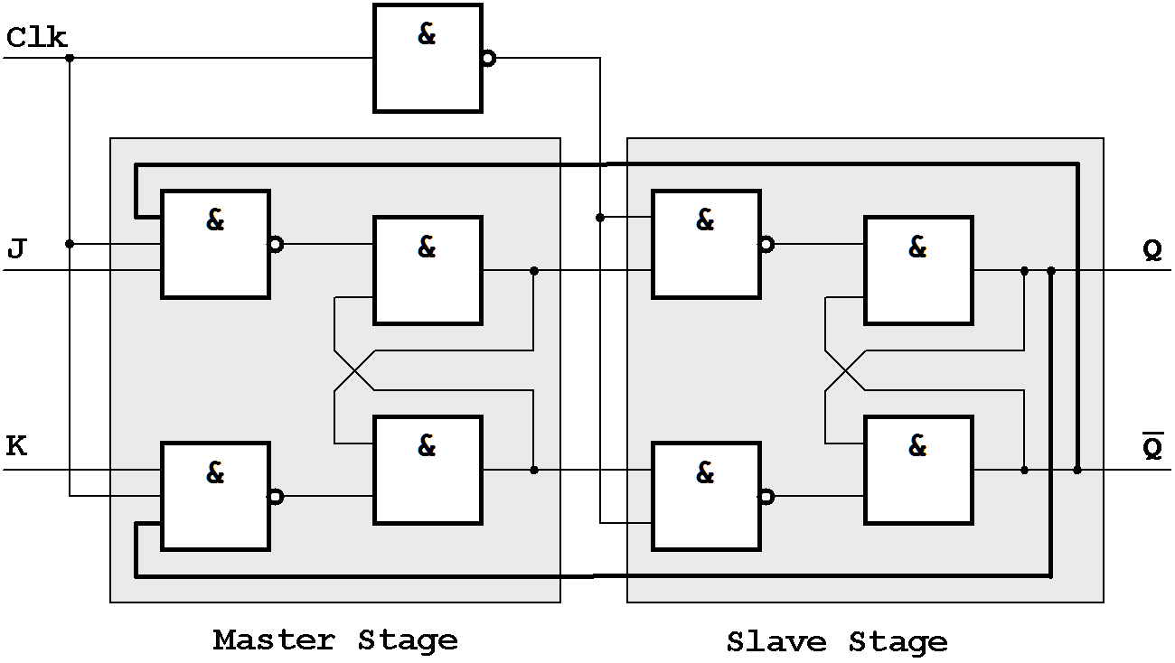
Figure 4.30: JK Master-Slave Flip-Flop.
With simple single-edge triggering it is possible to operate limited synchronous circuits, i.e. circuits in which a single signal is used to clock several flip-flops.
But when circuits are getting more complex with long clock lines, the signal propagation delay time has to be taken into consideration. Errors can occur because due to signal propagation delays not all flip-flops will be triggered at the same time. This time shift between clock signals is called clockskew.
Example:
In a simple serial connection of two D FFs the clockskew causes non-synchronous triggering:
Circuit:
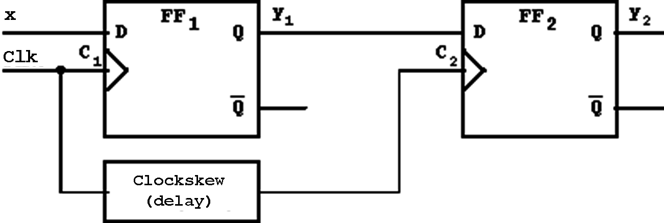
Figure 4.31: Flip-Flop Circuit with Clockskew Problem.
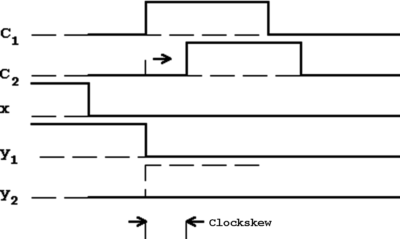
Figure 4.32: Temporal behaviour of the signals defined in Fig. 4.31.
In this example circuit the flip-flop FF2 shall assume the "1" level of y1 (see timing diagram). With the leading edge FF1 acquires the new "0" level, which will be output at y1 before FF2 will be triggered with the clockskewed signal C2 (Fig. 4.32). That means that FF2 will already receive the new value "0".
Result: y2 = 0 (expected value: y2 = 1)
This clockskew problem can be avoided to a large extend using so-called "dual-edge triggered" Flip-Flops.
In order to make edge-triggering possible, the "Master/Slave" configuration of two clock level controlled FFs was introduced. In a similar approach dual-edge triggering can now be achieved connecting two single-edge triggered FFs in Master/Slave mode:
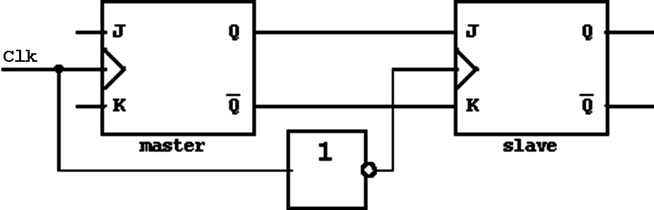
Figure 4.33 Dual-Edge triggered Flip-Flop.
In the dual-edge triggered flip-flop constructed this way the information is entered with the leading clock-edge and finally passed to the output with the trailing edge.
The time between clock leading and trailing edge serves to bridge the clockskew.
|
Figure 4.34: Circuit Symbol (DIN 40700, part 14) |
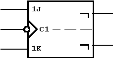 |
| Symbols: | |
| 1J,1K | indicate the time dependence of the inputs of C1 |
 |
Active: trailing edge of pulse |
 |
detailed (retarded) output |
From the edge-triggered JK Flip-Flop other types of flip-flop types can be derived (as has been shown in a similar way for the RS FF). From the multitude of FF derivatives especially the D Flip-Flop and the T Flip-Flop have special importance. The edge-triggered D FF corresponds in its function to the level-triggered D FF (see above), the T or Toggle Flip-Flop takes advantage of the toggle (change) function of the JK Flip-Flop.
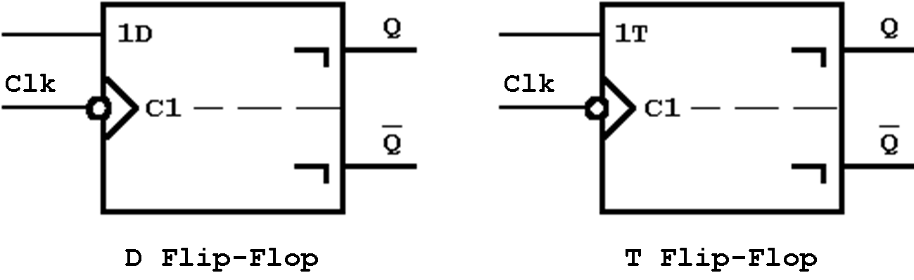
Figure 4.35: Circuit Symbols of the D and T Flip-Flops (dual-edge triggered).
 |
||||||
Table 4.7: Function Tables of the D and T Flip-Flops.
Note:
For the information transfer of the Flip-Flop (Latch) to work in a reliable way, the standard FF devices have to observe certain (minimal) timing conditions very precisely. These restrictions especially refer to timing definitions known as "setup time"
and "hold time", respectively. In connections with some devices also the so-called "rise time" and "fall time" of the clock pulse have to be considered.
Example: D Flip-Flop
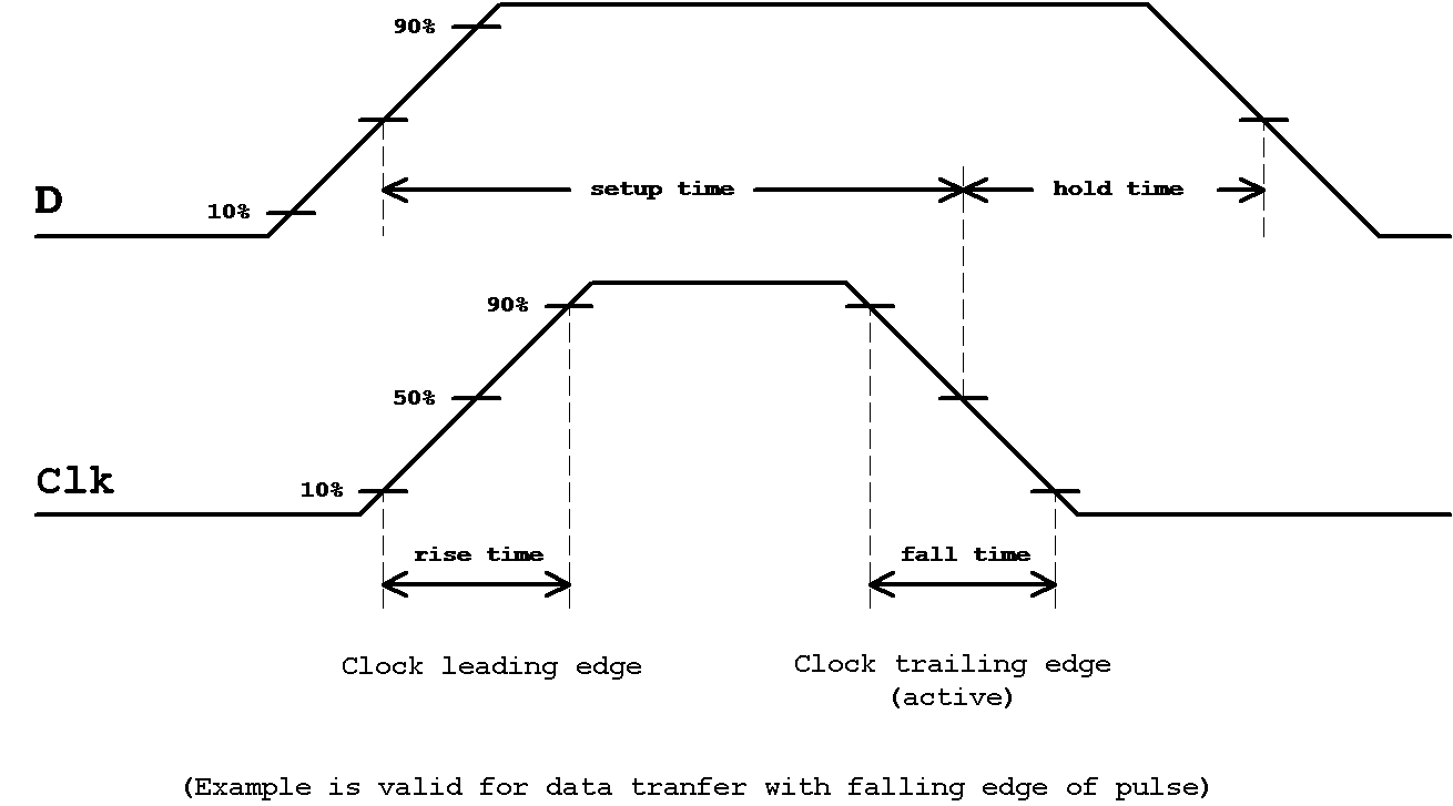
Figure 4.36: Pulse Characterization.
For devices of the 74LS family typical values for the "setup time" tsu and the "hold time" th are approximately:
| tsu | > | 20 ns |
| th | > | 5 ns . |
In most integrated Flip-Flop devices additional inputs for special control signals exist beyond the general inputs for the already known signals.
The standard Flip-Flop SN7474 (Dual leading-edge-triggered D Flip-Flop) for instance provides the asynchronous (clock-independent) input signals "preset" and "clear" used to program a well-defined initial state.
Both signals are active at level "0" (active low) and set the Q-output to "1" or "0" level, respectively.

Figure 4.37: Clock circuit diagram of the D Flip-Flop SN7474,
with preset
 , clear
  ,
clock CLK (clock signal) and Data input D.
,
clock CLK (clock signal) and Data input D.
|
 |
||||||||||||||||||||||||||||||||||||||||||||||||
Figure 4.38: Function Table (left, X = don't care) and Circuit Symbol
(right) of the D Flip-Flop SN74x74
(each device contains two flip-flop units).
In the English literature a clear distinction is made between flip-flops that are level-sensitive and edge-triggered, respectively, using the terms latch and flip-flop.
Although they are very similar, the two devices show quite different behaviours. A comparative example will clarify the difference:
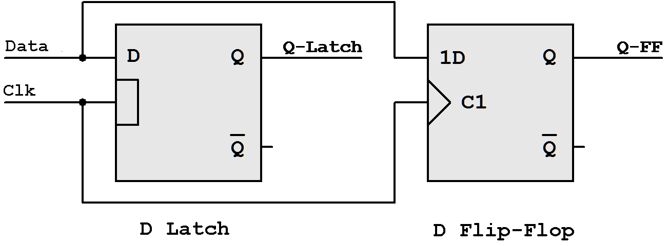
Figure 4.39: Example Circuit (latch, flip-flop).
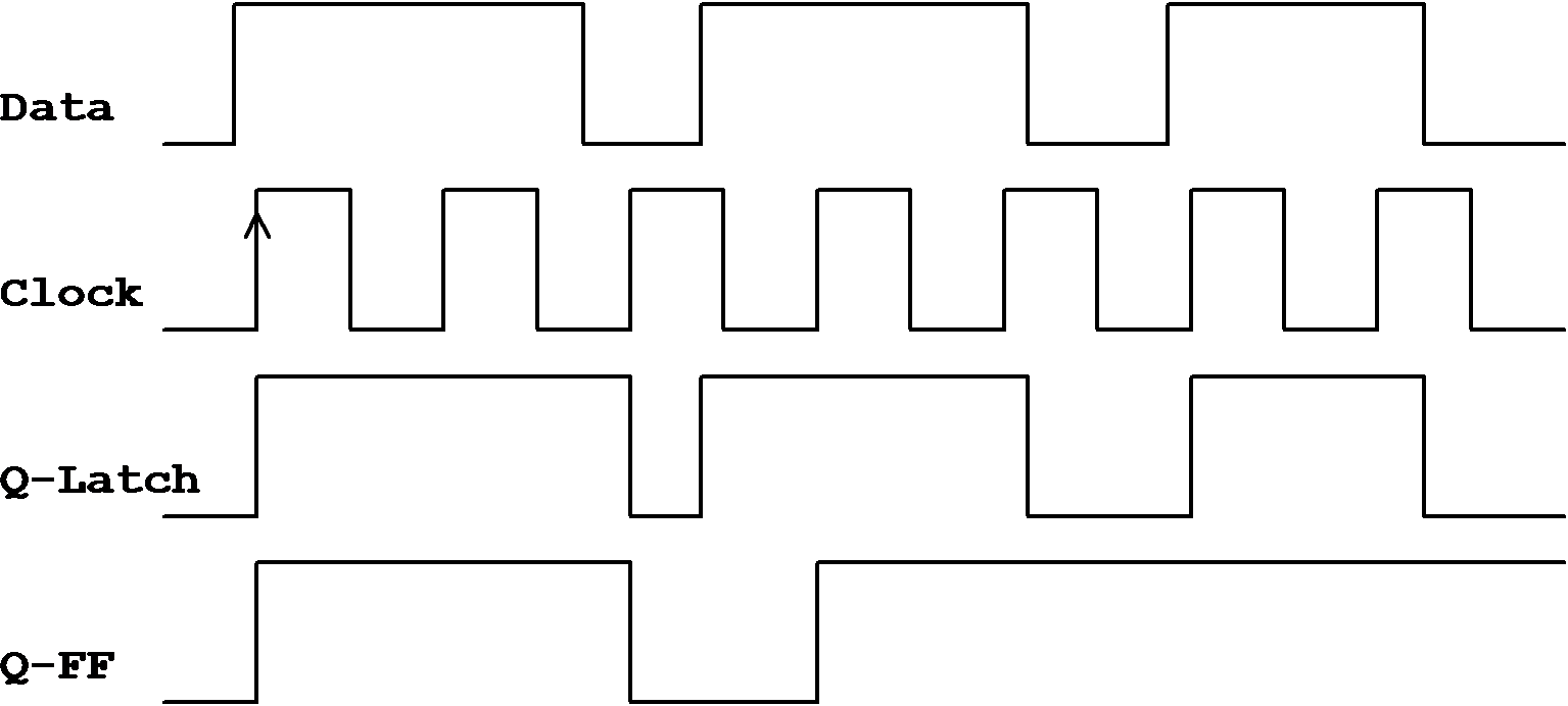
Figure 4.40: Timing diagram for circuit of Fig. 4.39 (not considering propagation delays).
Note:
The edge that is responsible for triggering the D Flip-Flop is indicated by an up-arrow "↑" (in this case the rising edge of the clock pulse is the active one).
4.4.9 Summary: Flip-Flop Classification
(no data) | |||||
 |
|||||
 |
 | ||||
controlled |  |
 | |||
controlled |  |
 |  |
||
triggered |  |
 |  |  |
|
triggered |  |
 |  |  |
|
Table 4.8: Summary of the standard Flip-Flop types.
As is shown in Tab. 4.9 the clock input can furthermore be expanded, in order to distinguish between a positive (rising) and a negative (falling) edge:
Clock Input with level-control. The input variables that depend on C will be activated when C = 1. |  |
Clock Input with edge-control. The input variables that depend on C will be activated on a "0-1"- transition (positive edge). |  |
Clock Input with edge-control. The input variables that depend on C will be activated on a "1-0"- transition (negative edge). |  |
Transformation between different types of Flip-Flops and the creation of new types is possible, as long as two criteria are observed:
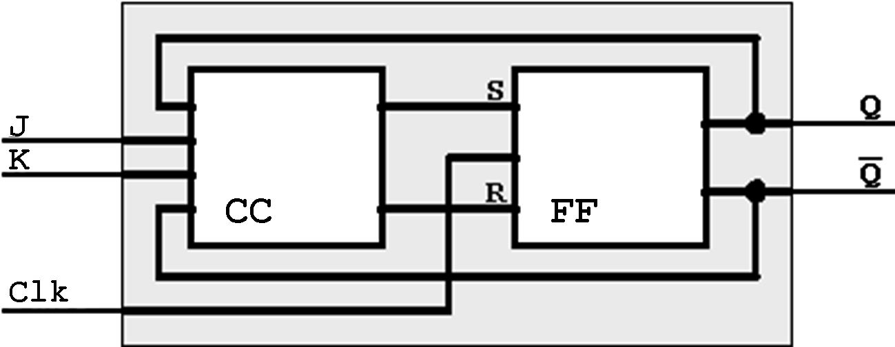
Figure 4.41: Example showing RS to JK Flip-Flop Transformation.
The required combinational circuit CC can be derived using the known methods. The sought-after flip-flop can be described using a function table, the standard flip-flop used for the implementation can be defined in the corresponding transition table. Fig. 4.41. shows the circuit structure for the transformation of an RS Flip-Flop to a JK Flip-Flop.
Table 4.10 compares the transition tables of the JK Flip-Flop and the RS Flip-Flop in the already introduced short form.
Table 4.10: Transition Tables of the RS and JK FFs.
Tab. 4.11:
Comparison of the complete transition tables for the JK and RS Flip-Flops.
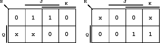
Figure 4.42: K-Maps for the determination of the JK/RS combinational circuit.
From the K-Maps the functional dependence of S and R from J, K, and Q can be derived:
| (4.7) |
| . | (4.8) |
From this the complete circuit shown in Fig. 4.43 results:
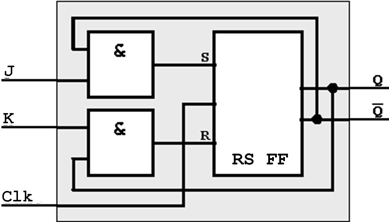
Figure 4.43: RS Flip-Flop wired as a JK Flip-Flop.
| Contents | Previous Chapter | Next Chapter |


