|
|  | ||
 | |||
 | |||
 |
Figure 4.44: Shift Register Classes.
| Contents | Previous Chapter | Next Chapter |
With the feedback lines the element of storage was added to the combinational circuits. In principle the resulting flip-flops represent storage units with a capacity of one bit.
Larger storage (memory) units can be realized using several flip-flops. In the most simple form the storage units built with a limited number of FFs is called a "register". Significant for these registers is that all registers involved are clocked synchronously (at the same time) using one unique clock signal.
Different types of registers can be implemented interconnecting the required number of FFs. The way the data inputs and outputs are used will determine the register type and function. With each clock signal information inside the registers will be moved bit-by-bit. Therefore the term shift register (abbr. SRG) is commonly used for this circuit type.
Considering their functions the following shift registers can be distinguished:
|
| | ||
| |||
| |||
|
Figure 4.44: Shift Register Classes.
For the implementation of shift registers all flip-flop types can in principle be used. Very often applied are especially the D and the JK flip-flops (the level as well as the edge sensitive ones).
Example:
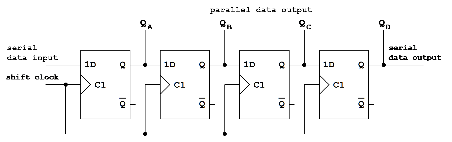
Figure 4.45: Realization of a right-shifting register.
Complete shift registers need additional control inputs beyond those that have been introduced so far, p.ex.:
When the connection between the Q output of one stage and the D input of the following FF stage is done not directly but via a multiplexer, then the programming of different SRG types becomes possible:
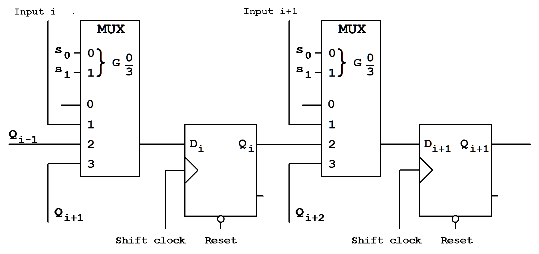
Figure 4.46: Shift register implementation with multiplexer support.
The functions of the control inputs s0 and s1
are then defined as follows:
| without function | ||
| parallel Load | ||
| right shift | ||
| left shift |
Table 4.12: Definition of the control inputs defined in Fig. 4.46.
Example:
Timing diagram and function table for the 4-Bit Shift Register shown in Fig. 4.45.
Requirements:
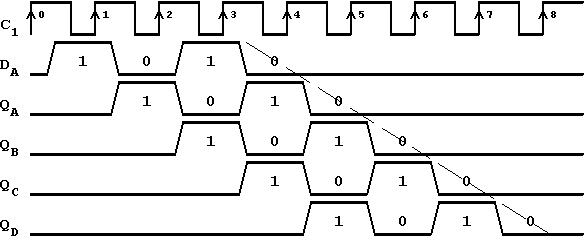
Figure 4.47: Timing Diagram (timing schedule)
Table 4.13: Function Table
(The darker fields correspond to the dashed line in the timing diagram)
4.5.3 Shift Register Devices (Integrated Circuits - ICs)
Example of a modern SRG device:
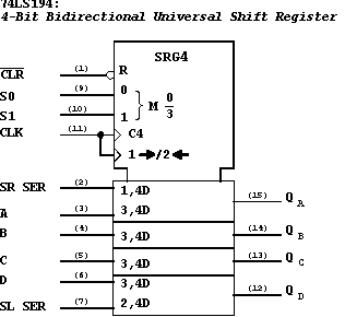
Figure 4.48: Integrated SRG Device (74LS194).
| Contents | Previous Chapter | Next Chapter |