Figure 4.4: Simple Timing Diagram of a Flip-Flop.
| Contents | Previous Chapter | Next Chapter |
The most elementary class of Sequential Logic Circuits is formed by the so-called
"Flip-Flops" (Abbreviation "FF"). Contrary to the combinational circuits the devices are characterized by the existence of an internal storage. Because of this memorizing ability the knowledge of the current input states is not sufficient in this case to describe the complete function. The current state of the internal storage must also be known (which essentially refers to the activity "history" of the device).
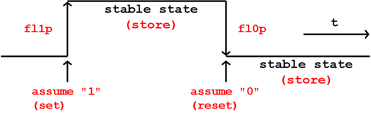
The most simple Flip-Flop circuit shall be characterized by the following three functions:
These three FF functions can be shown in a simple timing diagram:
Figure 4.4: Simple Timing Diagram of a Flip-Flop.
Flip-Flops can be considered fast electronic switches, that can for instance be used to keep the inputs of a combinational circuit stable, until all signal changes have passed through:
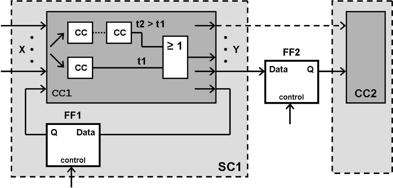
Figure 4.5: Flip-Flop Application.
The "switches"
FF1 and FF2 have to fulfil certain requirements as a prerequisite for a failure-free behaviour of the above circuit:
Observation:
In the typical Flip-Flop application shown here, the identifier X and Y refer to so-called bus systems, i.e. a collection of equivalent signal lines to one connection bundle. This "bundle" can for instance combine 8 lines and therefore carry 1 byte of signals. The flip-flop FF2 is available in a corresponding number (1 flip-flop per signal).
This configuration using Flip-Flops (FFs) in a parallel setup is called a "Register".
Obviously the Flip-Flop FF2 is part of a register. Functioning like an input switch for the combinational circuit CC2 it receives the output signals from CC1 and keeps them stable. Consequently the signals can propagate through CC2 while in CC1 a new "signal vector" is already evaluated. The individual results can even be produced at different times.
Because of the register (FF2) the input values of CC2 are not affected by any signal changes.
When the FF register remains in its storage position this will prevent the propagation of noisy signals produced in CC1 to CC2.
Obviously the same considerations are valid for the inputs of CC1 and therefore also for the feedback signal. This feedback can be interrupted by Flip-Flop FF1 whereby the timing behaviour will be changed. CC1 in connection with FF1 can be considered a new sequential logic circuit SC1.
In case that at the input of CC1 new values should only be accepted when all previously triggered signal waves have faded away, FF1 must block all feedback signals up to the longest propagation time in CC1 (delay time tD).
From this application the fundamental requirements that a basic flip-flop has to fulfil can directly be derived. The following timing diagram summarizes the required temporal and logical behaviour of the flip-flop:
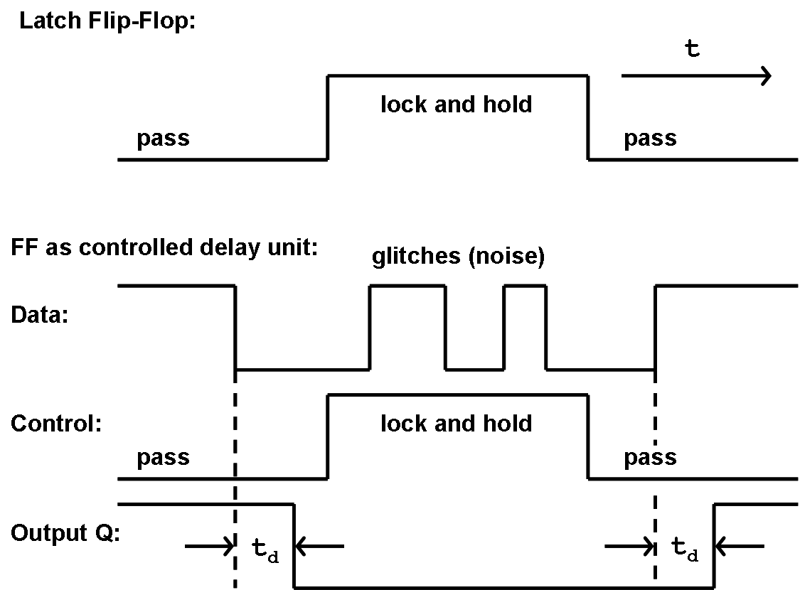
Figure 4.6: Timing and Logic Behaviour of a basic Flip-Flop.
An approximate solution would be possible with a dual-edge control, in which a programmable delay time
td should exist between the transfer of information with the flip-flop and the information output:
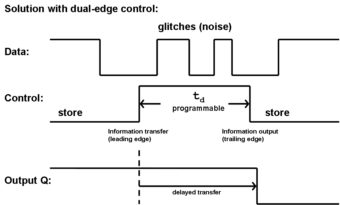
Figure 4.7: Dual-Edge Control.
4.2.1 Design of a Latch Flip-Flop
As a simple example a hypothetical Latch-FF will be developed first. This flip-flop shall be characterized by two distinguishable states:
For this flip-flop the circuit symbol below (hypothetical as well) could serve for a full description:
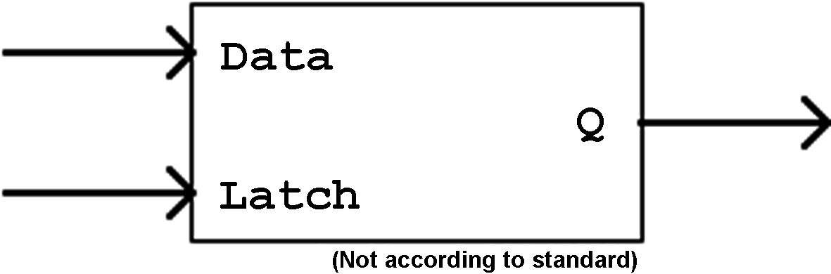
Figure 4.8: Hypothetical FF Circuit Symbol (not according to standard).
A tabular functional description (function table, truth table) can also be developed:
| 0 (unlatch) | (d = data) | ||
| 1 (latch) | (x = don't care) |
Table 4.2: Truth Table of the Latch Flip-Flop.
In the K-Map stable and non-stable states can directly be distinguished:
| Figure 4.9: K-Map of the Latch Flip-Flop. | 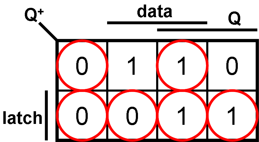 |
When Q+ indicates the state of the FF after the change of the input parameters, then obviously the following "store" and "hold" conditions will be valid:
| . | (4.1) |
The stable states have been circled (in red) in the K-Map.
This description becomes even clearer using the state diagram (state transition diagram) introduced before (see above):
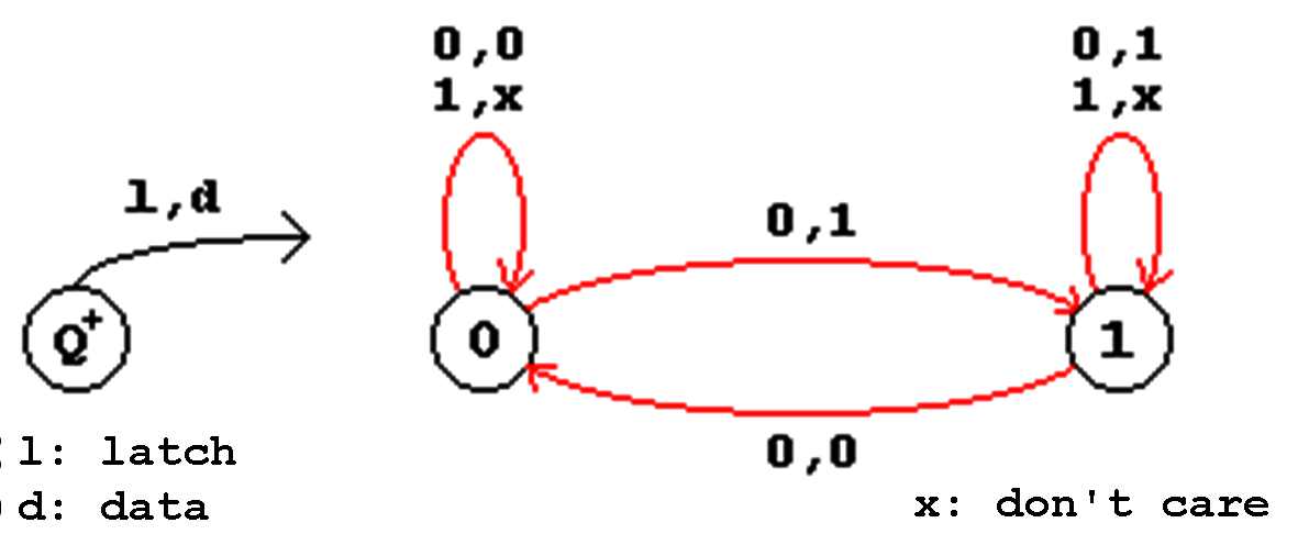
Figure 4.10: State transition diagram of the Latch Flip-Flop.
From the state transition diagram can be seen that this circuit has only two stable states, into which in can be transferred applying the corresponding input signals. Because of this property this circuit is also know as a "Bistable Flip-Flop".
A typical gate implementation of this flip-flop shows clearly the storage function implemented using a feedback structure:
| Figure 4.11: Gate Implementation of a Latch Flip-Flop (hypothetical). |
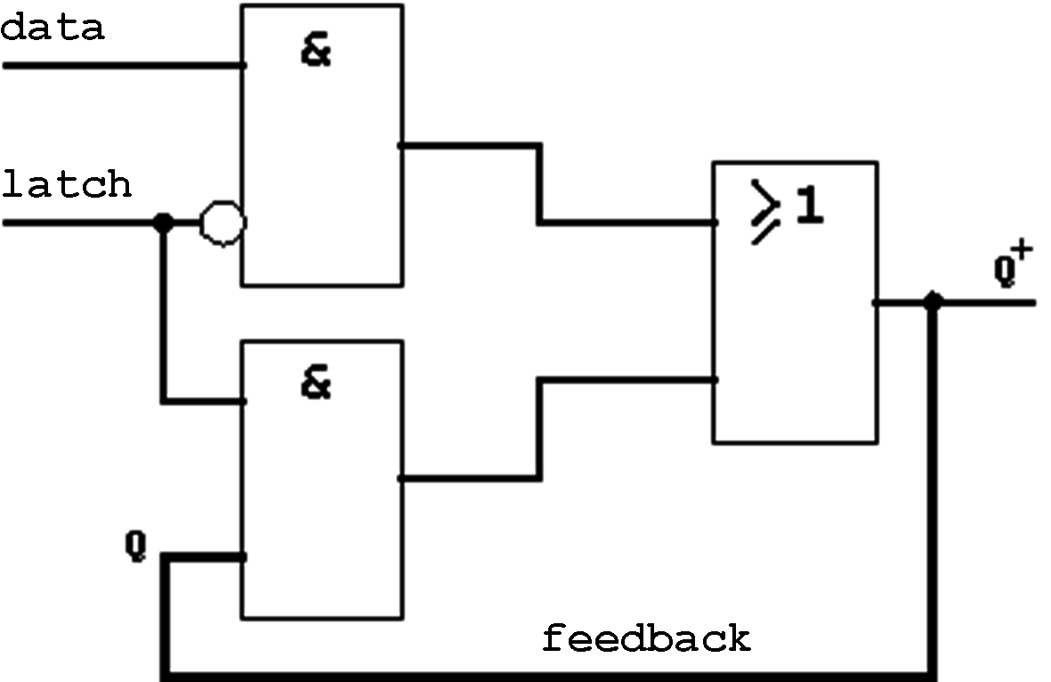 |
Function describing the Latch Flip-Flop:
| (4.2) |
| Contents | Previous Chapter | Next Chapter |