Figure 3.16: Basic PLA Structure
| Contents | Previous Chapter | Next Chapter |
As has been seen in the last chapter, the pure minterm decoding is a disadvantage in memory-based circuit realization, because it allows only the formation of complete conjunctions. In the so-called "Programmable Logic" this limitations does not exist anymore. This form of digital logic allows the formation of implicants as well as the consideration of "don't care" cases.
The circuit families that have these properties are summarised under the name PLD - programmable logic device. Especially three closely related device groups can be distinguished in this case:
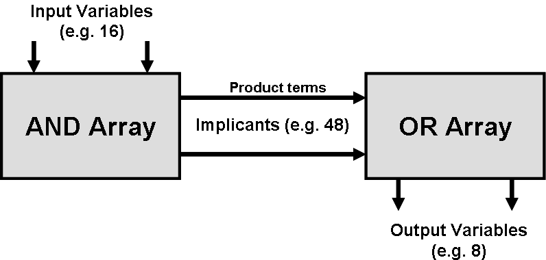
The "Programmable Logic Array" is based on the known AND/OR-Structure with the additional possibility, to not only produce minterms in a given AND array but to also allow the formation of larger field combinations:
Figure 3.16: Basic PLA Structure
The typical PLD device is characterized by an input structure consisting of AND gates and an output structure based on OR gates. The number of signal connections is programmable for both structures. Thus it can be decided which input signals can be connected with the AND gates and which product terms (implicants) can be connected with the OR gates.
This version of the PLDs in which both structures can be programmed is called "PLA (FPLA). The signals that are programmable, i.e. that can be interconnected, are combined in the form of arrays.
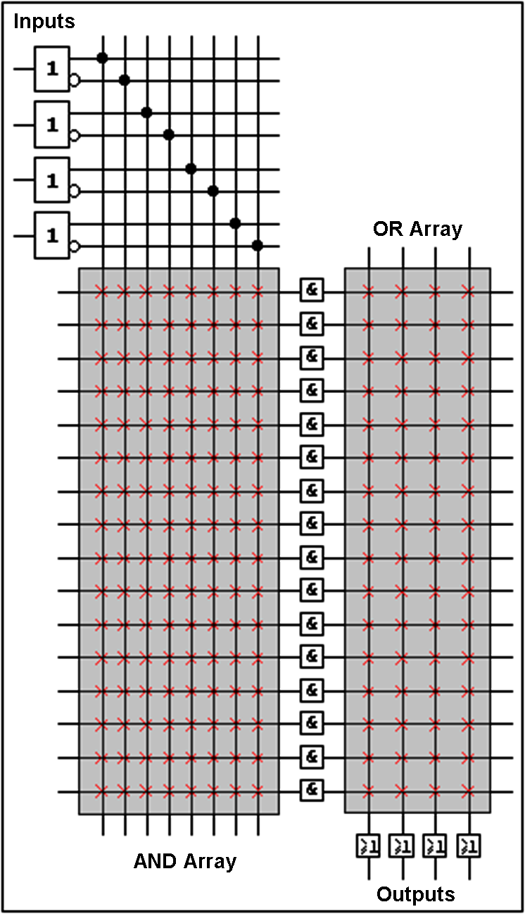
Figure 3.17: General PLA Structure
The connections (cross point switches) that are shown in this generic structure exist in the normal state of the PLDs. But as the following figures show they can be programmed by virtue of built-in "fuses" (fusible
links). This means that the connections that exist in both arrays can be cut off. The selective interruption of these interconnections is what is referred to as "PLD Programming".
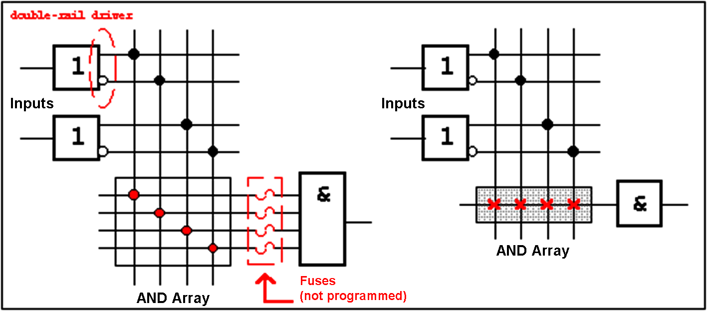
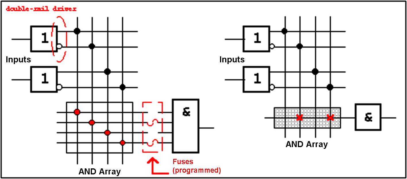
Figure 3.18: Detail showing PLA Programming
(not-programmed PLA, programmed PLA)
These PLA circuits exist in two special forms, in which only one of both array structures can be programmed, respectively.
When only the AND array can be programmed it is referred to as PAL device, in the case of a programmable OR array as the already known PROM device, which can be considered a special PLA case:
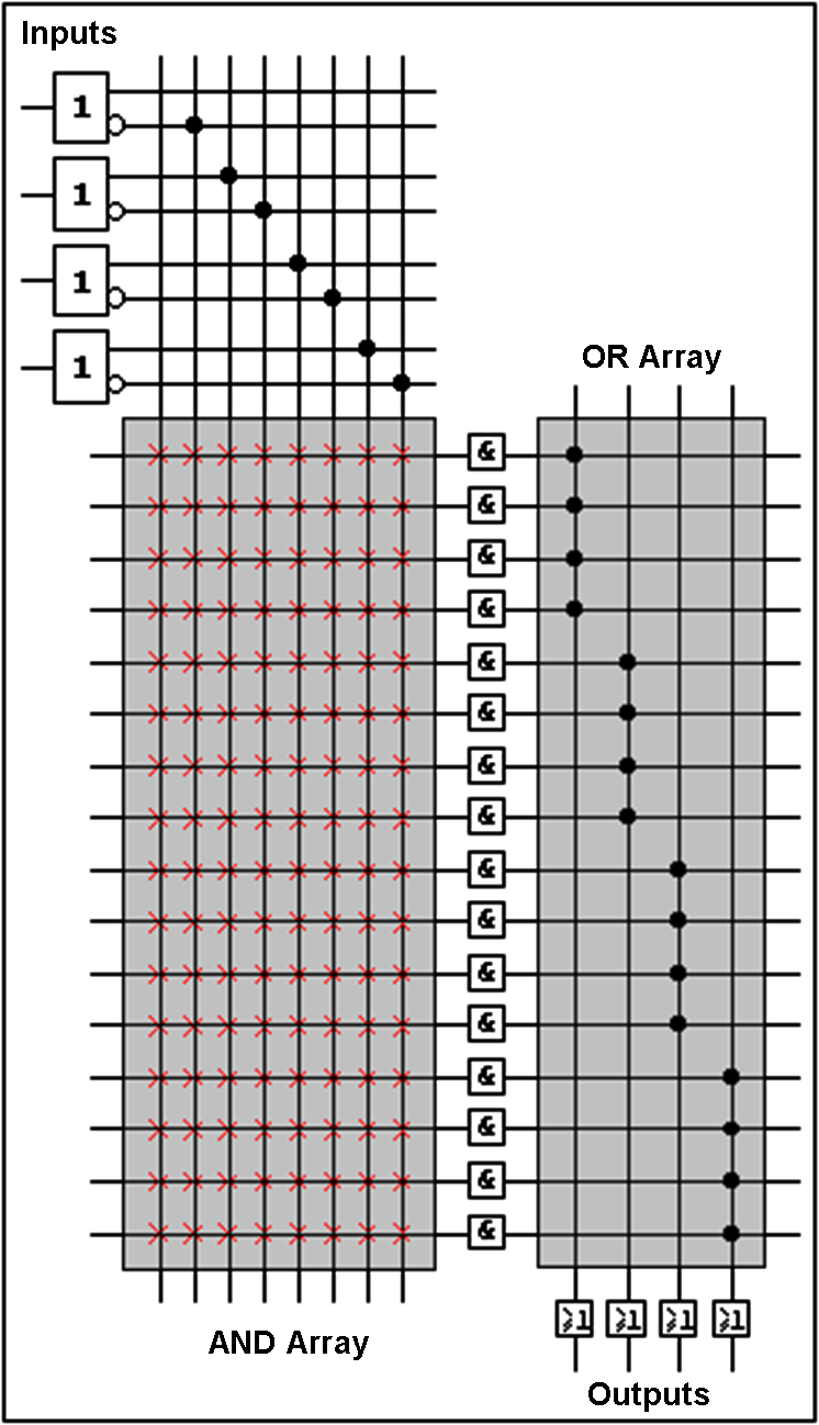
Figure 3.19: Programmable Array Logic (PAL) with programmable AND Array.
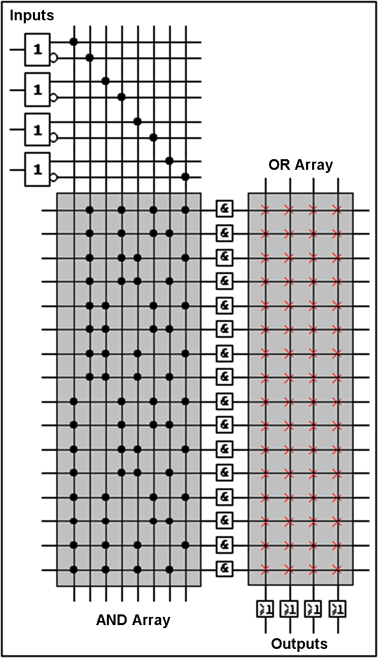 Figure 3.20: Programmable Read Only Memory
(PROM) with programmable OR Array.
Figure 3.20: Programmable Read Only Memory
(PROM) with programmable OR Array.
Obviously the three groups of programmable devices can be distinguished according to the programmability of their AND and OR arrays, respectively.
| PLA (FPLA) | programmable | programmable | |
| PROM (PLE) | fixed | programmable | |
| PAL | programmable | fixed |
Table 3.4: PLD Devices.
In order to clarify the difference between PLA and PROM, the application of these devices will be discussed in a typical example.
Two given functions x and y, described using truth tables, will be implemented using a PLD device:
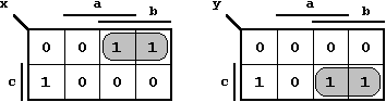
Figure 3.21: Functions x and y defined by a truth table (top), and corresponding K-Maps (bottom).
In this K-Map the possible simplifications have already been done, i.e. all group combinations are formed (implicants, product terms).
At first the function will be implemented using a PROM device:
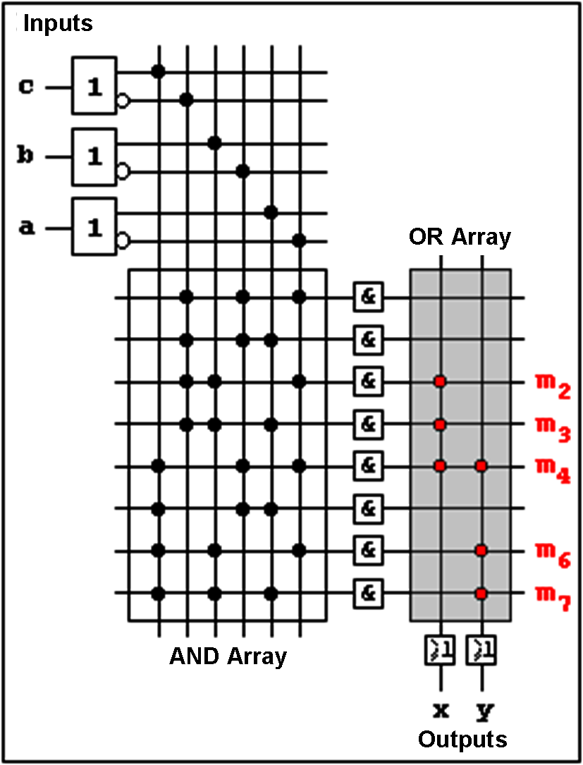
Figure 3.22 PROM Implementation of Functions y and y.
In this PROM realization only full conjunctions can be formed. The required minterms mi are indicated. In this example the minterm m4 can be jointly used by both functions (function bundle).
In the corresponding PLA implementation the implicants formed in the K-Maps can now be applied:
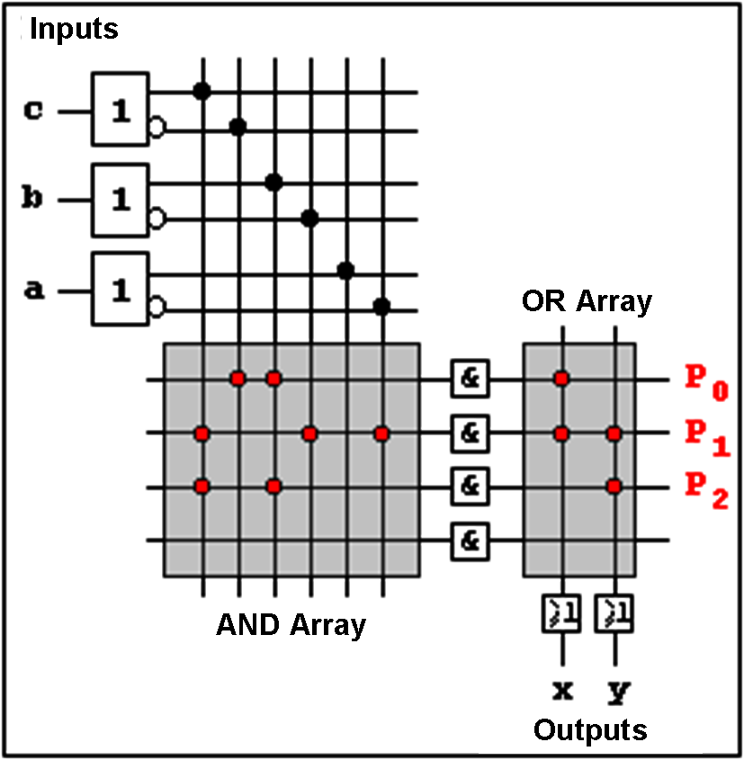
Figure 3.23 PLA Implementation of Functions y and y.
Of the three product terms
 | (3.3) |
P1 is again used by both functions. This term represents a full conjunction, i.e. it is identical to the minterm m4 in the above PROM implementation.
Considering the possibility to form implicants, the PLA realization requires fewer product terms than the PROM realization.
Therefore PLA and PROM devices are prepared for practical applications in such a way that two usable areas can be distinguished:
Typical values for these two parameters are:
| PROM (PLE) | ||
| PAL |
| Contents | Previous Chapter | Next Chapter |