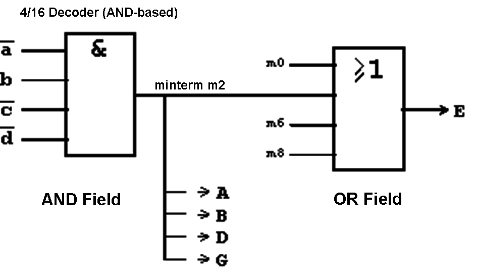
Figure 3.15: Representation of the minterm m2 and a subfunction of the output function E.
| Contents | Previous Chapter | Next Chapter |
Several approaches exist to solve digital design problems. Some of those have been treated, so far.
Especially three methods can be distinguished because of their importance:
When the Boolean Function is given, then the relation between input and output values is clearly defined, the circuit can be described in tabular form using a truth table. The most simple form to realize the circuit means just transferring the table to a memory device.
This leads directly to the method known as "Programmable Logic". The special circuits available for this purpose are summarized under the term PLD (programmable logic
device).
Using the problem of BCD Code to 7-Segment Code conversion (see above), the memory-oriented solution can be explained. For this purpose the input variables representing the BCD-Code are interpreted as addresses of the memory device. The 7-segment code represents the memory content.
Figure 3.14: Memory Allocation for BCD Code Conversion.
To store the complete table content in a memory device, obviously a memory capacity of 16 * 7 bits is needed.
The BCD-code is not complete. Therefore the input range for addresses 10 to 15 can be specified as "don't care" range, which in this case can be filled with '0' values.
Each of the seven Boolean Functions A - G of this table can be represented using a minterm decoding with subsequent OR-combination (see above).
Using memory address '2' and the output function 'E' this can be explained in detail:
To decode the input values (addresses) a simplified implementation is possible using an AND gate:
Figure 3.15: Representation of the minterm m2 and a subfunction of the output function E.
 produces the minterm m2.
As can be seen from the table, this minterm is necessary to describe the functions A, B, D, E and G.
produces the minterm m2.
As can be seen from the table, this minterm is necessary to describe the functions A, B, D, E and G.
To describe the function E the minterms m0, m6, and m8 are also required. They can be implemented using equivalent decoder realizations (AND gates). Finally E can be formed using an OR-combination of all involved minterms:
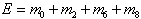 | . | (3.2) |
Thus the relation of the memory-oriented presentation of the function to the minterm-representation treated before is established.
Solutions of this type using read-only memories (ROMs) have advantages and disadvantages:
Advantages:
Disadvantages:
Especially the fact that neither the introduction of "don't care" positions nor the formation of implicants are possible, can be considered a big drawback.
| Contents | Previous Chapter | Next Chapter |