|
|||||||||||||||||||||||||||||||||||||||||||||||||||||||||||||||||||||||||||||||||||||||||||||||||||||||||||||||
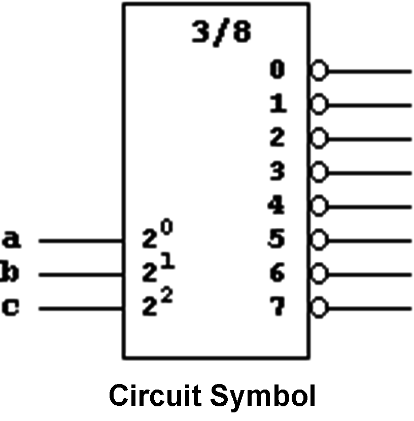
Figure 3.8: Circuit Symbol and Truth Table of the "1-to-8" Decoder.
| Contents | Previous Chapter | Next Chapter |
The inverse function of a multiplexer is done by a "Demultiplexer".
Related to the demultiplexer but constructed in a simpler way is the so-called "Decoder", which will therefore be discussed first.
The basic function of a decoder is to transform a code that implements 2n states into a "1-of-n" presentation. This "1-of-n" code is realized by activating one single signal out of a group of 2n signals. A typical example for such a transformation is the conversion of a binary number into a "1-of-n" code.
Using truth tables this can be easily demonstrated:
Example: Decoding a 3-bit number into a "1-of-8" code
Figure 3.7: Converting the Binary Code into the "1-of-8" Code.
More common is the decoder realization with output signals that switch to level "0" when active ("active low"):
|
|
|||||||||||||||||||||||||||||||||||||||||||||||||||||||||||||||||||||||||||||||||||||||||||||||||||||||||||||||
Figure 3.8: Circuit Symbol and Truth Table of the "1-to-8" Decoder.
Decoders are frequently used for the selection of other circuits (see below). In order to facilitate this application, they are in most cases equipped with complex "Enable"- inputs. This type of circuit only works as a decoder when the corresponding Enable functions are activated.
Example:
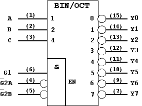
Figure 3.9: Decoder Circuit 74LS138 (Symbol according to ANSI/IEEE, IEC, DIN).
This device has three "Enable" input lines. The decoder is activated when:
Is just one of these conditions not fulfilled, the device will enter the passive mode (via AND function), i.e. all outputs will be switched to the "1" level.
 |
 |  | |||||||||||
Table 3.1: Truth Table for the Decoder 74LS138.
With a small modification the Decoder can be transformed into a Demultiplexer. This modification does not change the basic construction of the device, it just means a different interpretation of the corresponding inputs and outputs.
The task of the demultiplexer is to switch (distribute) an information (data), that is received on a single signal line, to one out of 2n possible output signal lines.
The decoder comprises only the n selector inputs (a,b,c) for address selection. But it is possible to interpret the highest selector input as a data input, e.g. the input c.
Now only the selector inputs a and b are available, which has the consequence that only four decoder output lines are used (0 - 3), the remaining outputs (4 - 7) are not used.
When the highest address input of the decoder is used as a data input line, then obviously:
As can be seen, the device works as a demultiplexer.
A second possibility to use the decoder as a demultiplexer is the result of an extended use of the Enable inputs:
For instance, if the previously defined Enable input  is connected as a data input, while the other two Enable inputs remain activated, then:
 = 0:
signal level at the selected output Yi : "0";
= 0:
signal level at the selected output Yi : "0"; = 1:
signal level at the selected output Yi : "1".
= 1:
signal level at the selected output Yi : "1".Obviously in this case too the decoder works as a demultiplexer.
In order to emphasize the function of the demultiplexer, the circuit symbol of the decoder is slightly modified in this application:
Example:
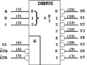
Figure 3.10: The Device 74LS138 as a Demultiplexer (DEMUX)
(Circuit Symbol according to ANSI/IEEE, IEC, DIN).
In many applications (e.g. microprocessor systems) the so-called "addressing" is necessary. The term addressing refers to the specific selection of a given component (example: memory units, peripheral units, etc.) in a larger system, for instance to prepare a data transmission process.
In most cases several devices are connected to a single communication path, used for the desired data transmission. The connection to such a system can be done with devices that provide so-called Tristate outputs.
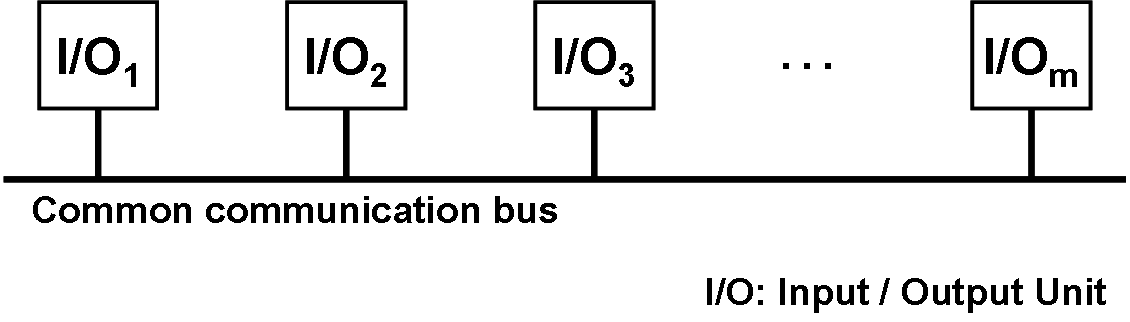
Figure 3.11: Typical Microprocessor Application.
To select (address) the I/O-unit (input/output) and enable it for transmission, a decoder must be employed, so that:
| m ≦ 2n | , |
| with: | m = total number of I/O devices, |
| n = number of decoder selector inputs. |
This results in the following decoder application:
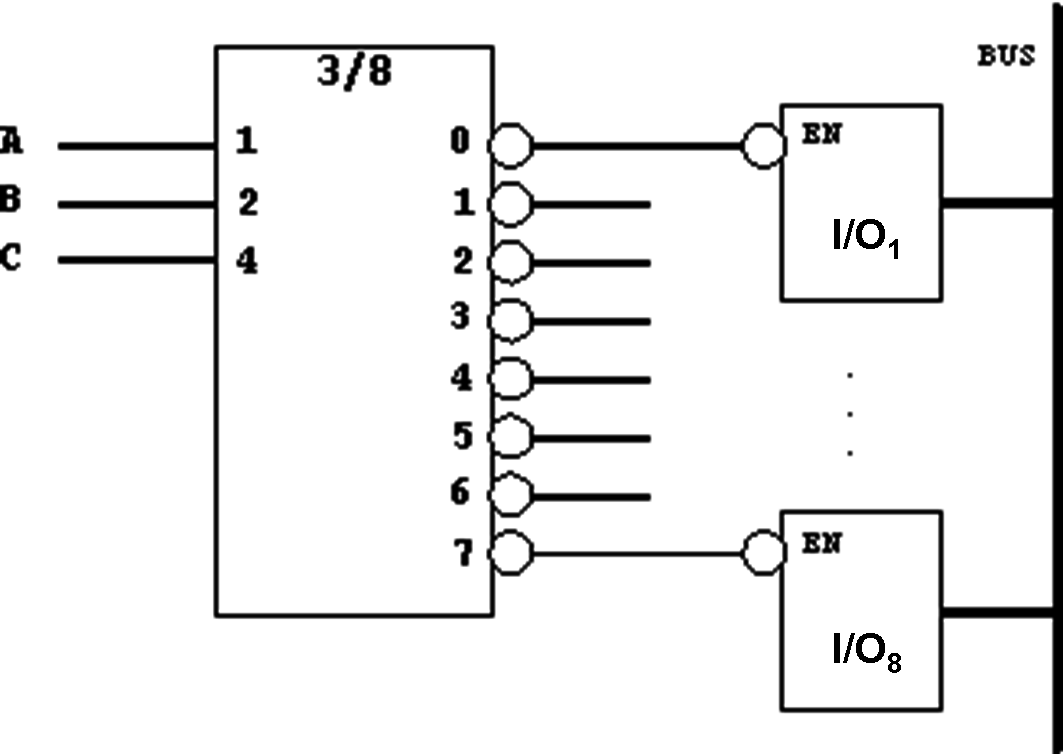
Figure 3.12: Decoder Application in Microprocessor Systems.
To complete the symmetry between multiplexer and decoder/demultiplexer, the decoders can also be used as universal logical blocks.
Table 3.3: Decoder (active low).
As can be seen from the above truth table for the "3/8"-Decoder, each of the eight decoder outputs produces a maxterm function M0 - M7. Accordingly a decoder with inverting outputs produces all minterm functions m0 - m7.
From this statement follows directly that every Boolean Function can be realized with a decoder block.
Application Example:
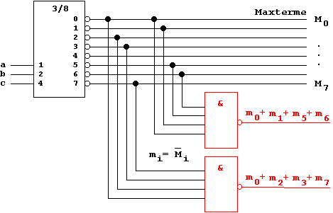
Figure 3.13: Decoder as Logical Block.
In this application circuit a "3/8" decoder with inverting outputs (active low) produces all possible eight maxterm functions. Using a NAND gate to connect these maxterms Mi, a cDNF is formed:
Correspondingly a decoder with noninverting outputs (active high) produces all minterms mi. With a subsequent OR gate the desired function is available in the form of a cCNF.
| Contents | Previous Chapter | Next Chapter |