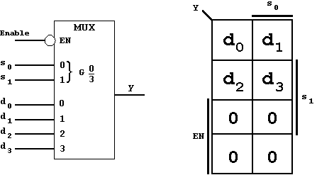
Figure 3.2: Circuit Symbol and K-Map of a Multiplexer.
| Contents | Previous Chapter | Next Chapter |
The following circuit symbol describes the 4:1-Multiplexer. The function can be shown using an 8-element Karnaugh Diagram.
Figure 3.2: Circuit Symbol and K-Map of a Multiplexer.
From the K-Map the Boolean Function can be derived:
| . | (3.1) |
According to their functions the multiplexer inputs can be divided into three groups:
The selector inputs select the data input which will be logically connected with the output Y. The Enable input has the function to enable or disable the complete operation of the multiplexer, in order to facilitate the co-operation (interconnection) of several multiplexers.
In the above example the Enable signal must be on the logic level '0' (active low), in order to enable the multiplexer.
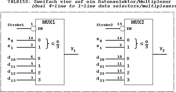
3.1.1 Multiplexer: TTL DevicesIn the so-called TTL family of logic circuits as well as other circuit families different multiplexer types are available.
The description introduced above refers to the TTL circuit 74x153 (depending on the circuit family used, x corresponds to "LS", "ALS",
etc.):
|
Figure 3.4: |
 |
As the name indicates, this TTL device contains two identical multiplexer units. Both multiplexer units have their own "Enable" input, called "Strobe" in this case. But the selector inputs s0, s1 are combined for both units. This means that in a practical application in both multiplexers always identical channels will be selected.
When the "Enable" signal is on level "1" the corresponding out "Y" of this device will be in passive mode, that means that it will assume "0". Obviously such a device cannot be used in a bus system. Furthermore it is not possible to distinguish between a passive output level and an actively transmitted "0" data level.
Other devices overcome this disadvantage applying so-called "Open-Collector" or "Tristate" outputs, whose advantages are especially important for bus-oriented application.
Example:
The circuits 74LS604/606/607
The devices are manufactured using LSI Technology (Large-Scale Integration), showing a much higher degree of complexity. They exist in versions with "Tristate" output (74LS604/606) and with "Open-Collector" output (74LS607), which makes their application in bus systems feasible.
On the input side these devices are connected with two data busses A and B, which are 8 bit (1 Byte) wide. The data are stored internally before they are connected to the output. This mode of operation, called buffered output, explains the identification of this devices as "multiplexed latches".
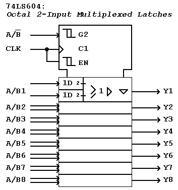
Figure 3.5: Byte-oriented Multiplexer Device..
Functional Description:
With the input line  the input bus gets selected. This device implements an 8-fold "two to one" Data Selector / Multiplexer. Therefore one selection signal is sufficient. The time of the data transfer and the output Yi are controlled by the so-called "clock" input "CLK". The rising edge (01) of this clock pulse determines the transfer of the data, that are stored and remain available at the outputs Yi as long as CLK = "1" is valid.
Description of Symbols:
 |
indicates "Schmitt Trigger" inputs (for noise reduction); | |
 |
indicates rising edge; |
|
 |
characterizes outputs as "tristate"; |
|
| 1D | indicates buffered transfer (D Flip-Flop), transfer with C1, the rising edge; |
|
| 2 | Input G2 is used for the selection of A/B. |
Amongst others the following devices belong to these groups:
| 74150 | Totem Pole | ||
| 74151 | Totem Pole | ||
| 74157/258 | Tristate | ||
| 74251 | Tristate | ||
| 74253 | Tristate | ||
| 74257/258 | Tristate |
|
# number of units per device |
Figure 3.6: Typical Multiplexer Devices.
| Contents | Previous Chapter | Next Chapter |