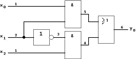
Figure 5.1: Sample Circuit
| Contents | Previous Chapter | Next Chapter |
Using a simple example circuit, the reason for the occurrence of time-limited errors in digital circuits can be demonstrated:
Figure 5.1: Sample Circuit
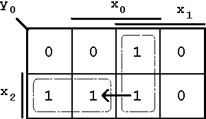
Figure 5.2: K-Map ref. to the circuit of Fig. 5.1.
 '0'
'0'
with constant values x0 = x2 = '1',
then a short signal change at output
y0 can be observed.
The timing diagram clearly shows that due to the inversion of signal 2 the signal 4 will be delayed by one gate delay compared to signal 5. Therefore at the input of the OR gate for a short time the unexpected case will occur, in which both input signals 4 and 5 are '0'.
Consequently output
y0 can be switched to logic '0' for the time corresponding to one gate propagation delay (in the following timing diagram a uniform delay time of 10 ns is assumed).
Figure 5.3: Timing Diagram.
The appearance of this spurious pulse (glitch) at the OR-output (signal 6) cannot be precisely predicted. Gates may "absorb" very short signals because of their internal capacities (see also: dynamic noise immunity).
Because of the circuit design (in this example) the danger of a delay-dependent erratic behaviour exists. This risk that may exist in a circuit realization is called a "Hazard".
Definition:
When a circuit structure allows during an arbitrary input signal change the appearance of a spurious pulse, then the circuit realization contains a Hazard. This pulse that occurs due to the hazard is called a glitch or spike.
Example:
The following example will show how decisive a hazard can be for the function of a circuit:
A combinational circuit will be used to produce the signals that are needed to control an RS Flip-Flop. The RS FF shall be maintained in the "Store" state (R=S='0' in NOR realization), but a glitch (hazard) occurs on the R line:
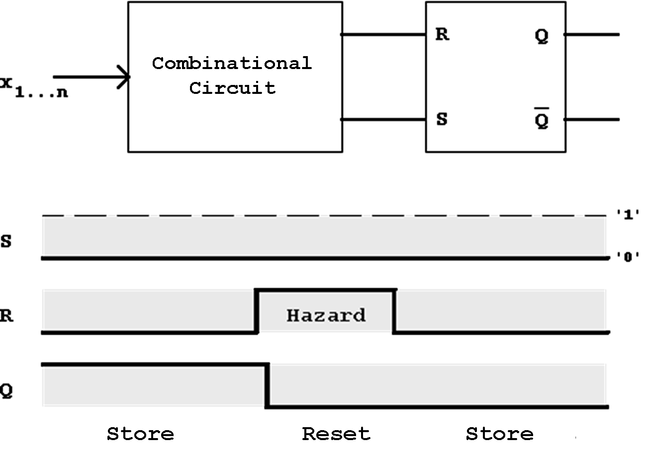
Figure 5.4: Hazard-caused erratic behaviour of a flip-flop.
The RS Flip-Flop indeed remains in the "Store"state, but the glitch generates an unwanted reset of the Q output.
The sources of these problems are erroneous circuit structures, their localization can be quite difficult. Very often a complete redesign of the circuit is necessary for the removal of these hazards.
| Contents | Previous Chapter | Next Chapter |